3D MID component carrier protects point of sale terminals
- Details
- Hits: 12342
Flexible circuit boards made of thin polyimide films have established themselves in many product areas. But they are complex to equip and assemble, even if they offer many advantages. Hence sets Harting auf die 3D MID Technology that can save up to two thirds of the costs. In one POS terminal it offers the highest physical protection against cyber attacks.

Content of the technical article
- 3D MID technology secures POS terminals
- 3D-MID technology at Harting
- Component carriers save two thirds of costs
- Further applications of the 3D-MID component carrier
- Explanatory video for the 3D-MID process
- What is 3D-MID technology?
3D MID technology secures POS terminals
 Point-of-sale terminals (POS) are inadequately protected against physical attacks. According to a survey by the digital association Bitkom, the scope and quality of cyber attacks have increased dramatically in recent years. In 70% of companies in Germany they caused damage amounting to 102,9 billion euros. "The hackers of the past have evolved into well-equipped and often technologically well-versed cyber gangs," says Bitkom.
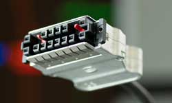
POS terminals are also among the targets of attack. Will be on them sensitive data temporarily stored such as credit card numbers and PIN codes in order to prevent data loss if the payment process is interrupted. Such data can be read by attackers by gaining access to the hardware with the help of probes or mini-drills. An additional security element can now reliably prevent data loss.
3D MID protective caps increase safety classification
 The electrical conductor tracks on the inside of the protective cap create a very reliable additional security element against physical attacks. They form a closed circuit and are so close together that an attacker can practically no longer gain access. An attempted attack would either damage a conductor track and interrupt the circuit or short-circuit two conductor tracks. This switches off the POS terminal immediately. The cached data is lost and the device is unusable.
Using 3D MID (Mechatronic Integrated Devices) The electrical conductor tracks are directly applied to the process Plasticparts of the protective caps applied. The circuit carriers manufactured in the injection molding process replace conventional solutions with a plastic carrier and printed circuit boards by integrating the function of both parts in an MID. The components are lighter and fewer and the production costs are reduced.
3D-MID technology at Harting

 Harting is that largest supplier of 3D MID components (Mechatronic Integrated Devices) outside of Asia and offers the complete value chain of 3D MID technology under one roof with development and prototyping of customer-specific products. These are manufactured using injection molding, direct laser structuring, metallization, assembly and connection technology and final testing.
Harting continues the whole 3D MID process chain in-house for over ten years from the project idea to the assembled series product. The technology is used in the production of Industrial electronics, Medical Technology, Entertainment electronics or for safety-relevant components of the Automotive industry.
Thanks to the technological edge of Harting's 3D MID technology, users benefit from compliance with the strictest Payment Card Industry Data Security Standard (PCI-DSS) requirements. The technology differs from other providers of security enclosures in that the conductor track widths are smaller. The closer the distance between the individual conductor tracks, the more difficult it is to manipulate the circuit. While most providers realize conductor track widths and distances of around 300 to 500 µm, the technology leader manages 70 to 150 µm.
In addition, the company is the only 3D-MID producer worldwide that has a Laser system with three fine focus optics disposes. The fine focus laser reduces the distance between the conductors to 70 to 80 µm. In this way, more conductor tracks can be placed on the component and the packing density increased. In addition, 3D MIDs allow more versatile shapes. For this purpose, flexible geometric contours are created in injection molding and then processed with a laser for the electrical conductor tracks. Rounded edges, elevations or transitions can be produced in this way.
Component carriers save two thirds of costs
 Be at Harting electronic components such as LEDs, ICs, or photodiodes Sensors automatically placed directly on the component carrier. The total costs for manufacturing the component carrier are two-thirds lower compared to flexible printed circuit boards. This cost advantage compared to the flexible printed circuit board results from the Eliminate the often complex handling in the form of loading, Glue and assemble.
Even at small quantities The process is worthwhile because the component carrier can be used unchanged for various applications. There is no need for a new injection molding tool. The components are also fitted more precisely and with greater repeatability.
Harting sees a further advantage in the shorter project duration until delivery of the finished components. Because the plastic carrier remains unchanged, the specifications for the placement of the electronic components are sufficient. Based on this, the experts for 3D MIDs create a production-optimized Layout suggestion. Only the laser program needs to be set up to adapt the electrical conductor tracks to the application. The first samples can be delivered in two to three weeks after approval by the customer and delivery of the components - if necessary, faster.
Further applications of the 3D-MID component carrier
 In the following, three further applications of the 3D MID technology are described as examples, in which the Component carrier replace the flexible circuit board can:
Components at a 90 degree angle to the circuit board
The 3D MID technology component carrier is suitable for applications in which electrical components such as Sensors at right angles to the circuit board should be positioned. Automatic assembly allows high accuracy when placing temperature and Hall sensors. This means that users receive exact and repeatable measurement results. Also optical components such as LEDs or photodiodes for precision Photocells can be installed like this.
Temperature sensor at a distance from the circuit board
The component carrier allows a distance between the circuit board and an electronic component. A temperature sensor can therefore be used for temperature measurement in the housing, without the measurement results being influenced by the waste heat from other groups of components on the circuit board. In this way, an LED can be placed at a distance from the circuit board. Possible shading of the surrounding assemblies are avoided.
Component carrier with individual antenna function
The component carrier can be produced with different base polymers. In doing so, electrical properties such as the dielectric constant and the loss factor of materials can be taken into account, which are suitable for antennas suit. The individual antenna layout can be used for various applications in the MHz and GHz frequency range. examples are 5G, Bluetooth, Wifi or Zigbee.
 Connectors for the three zones of the food industry
The assembled component carriers are in Blister belts Delivered on rolls (tape & reel). Like other SMD components, they can also be fitted automatically as a standard design. There are two sizes. Electronic assemblies with standard size SOIC-8 and smaller can be fitted on them. Harting also realizes customer-specific formats.
Explanatory video for the 3D-MID process
Technical expertise
3D MID (mechatronic integrated devices) are injection molded circuit carriers. The technology populates a three-dimensional base body directly with electronic components and does without the circuit board and connecting cable. The base body is manufactured using the injection molding process. The thermoplastic is provided with a non-conductive, inorganic additive. The additive in the plastic is "activated" by laser direct structuring (LDS).
 With Kuka from the Harting connector to robot connectivity
In this way, the injection molded plastic can accommodate electrical conductor tracks. The laser beam describes the areas provided for the conductor tracks. This is how one comes about micro-rough structure. The released metal particles form the cores for the subsequent chemical metallization. In this way, electrical conductor tracks are applied to the three-dimensional base body. The plastic has a high heat resistance. It can therefore be soldered in the reflow oven.
You might also be interested in...

industrial housing | Indoor and outdoor control boxes

Electrical Wires | From cable to assembly

RFID and Barcodes | Industrial identification

Ethernet switches | The data driver in the network

Reduce carbon footprint | That's how it's done!

Charging plug, charging cable | For the electric car

Thomas Hess is Head of Product Development + Technology Roadmap at Harting AG in Biel