Chemically nickel / gold surfaces for printed circuit boards
- Details
- Hits: 6367
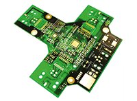 Beta Layout now offers HAL as a surface as well as chemical nickel / gold (Enig - Electroless Nickel Immersion Gold) for super flat pads in the PCB pool. With layer thicknesses of 4 to 8 µm nickel and 0,07 to 0,1 µm gold, the Enig surface is characterized by high planarity, good aging stability, suitability for soft soldering and bonding and as a surface for simple contact tasks. Electroless nickel / gold surfaces can be soldered several times and are often used in applications with very fine structures, which are becoming more common due to the miniaturization of components.
Here a particularly flat soldering surface is required. Unlike the shock-like heating in the HAL process, Chemical Nickel / Gold has no thermal stress that can lead to twisting and warping. In addition, this surface is RoHS compliant and has a shelf life of at least 12 months. Upon request, customers receive a paste stencil, an RFID chip embedded in an overdelivery and an 3D model of their assembled printed circuit board in advance for each prototype order.