1 mm² image sensor enables the world's smallest digicam
- Details
- Hits: 7815
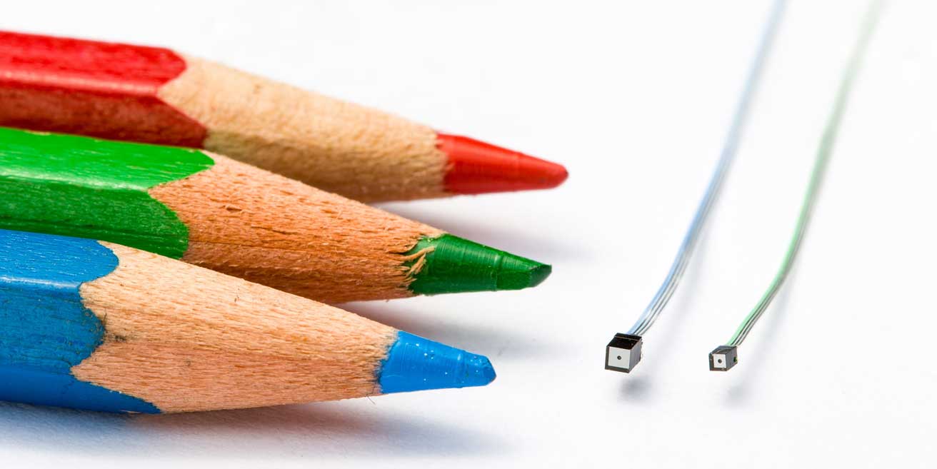
With an area of 1 mm², it is the world's smallest camera module Naneyem from AMS Osram via a fully digital output. The for the image sensor necessary Circuit board effect AT&S developed with the help of embedded component packaging technology. The mini digital cameras are suitable for wearables such as VR glasses or smartphones and for medical equipment. In this way, they are following the trend towards single-use endoscopes, which are particularly needed in bronchoscopy in the Covid-10 pandemic.
Content of the technical article
- Camera module for single-use endoscopes
- Camera module with chip on tip approach
- What is Embedded Component Packaging
Camera module for single-use endoscopes
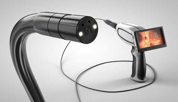 AMS Osram will be expanded Naneye portfolio the Naneyem camera module for medical single-use endoscopy. The high resolution corresponds to current market standards - but with the smallest available size in the field of digital endoscopy camera modules.
Endoscopic procedures such as bronchoscopy are currently seeing an acceleration in the transition from reusable to single-use bronchoscopes. Last but not least, the Covid 19 pandemic has one here increased demand triggered. The camera module was developed for single-use applications that guarantee a high level of sterility and reduce the likelihood of cross-contamination. The small dimensions of 1,0 x 1,0 x 2,7 mm enable the use of the Sensors in the smallest of spaces.
"Thanks to its space-saving size, the Naneyem is made for use in areas with severe size restrictions, such as single-use applications in bronchoscopy, urological endoscopy or endoscopic procedures in the kidney," says Dina Aguiar, Marketing Manager at AMS Osram. “The combination with the required high image quality makes it Cameras a unique and attractive solution for the rapidly growing market for single-use endoscopes. "
Manufacturer of the image sensor circuit board
The image sensor used is smaller than a grain of rice, lighter than a postage stamp, but more powerful than any image sensor of its kind that has existed to date. "The image sensor not only creates sharp images due to its resolution of 100.000 pixels, it also has a low power consumption thanks to our smart connection architecture," says Markus Maier, Global Account Manager at AT&S. The Austrian company developed the circuit board for the sensor. The developer of the sensor AMS Osram is a leading global provider of optical solutions, also headquartered in Austria. Both companies have already worked together on technology projects in the past.
 Cameras with CMOS sensors for medical technology and life science
The digicam sensor offers one digital video output and enables any kind of visual sensing for mobile applications of digital cameras. The Naneye camera module is one of the first products in which the circuit board is integrated. In addition to the world's smallest digital camera, the field of application of the image sensors is much broader. The sensors can be used, for example, for eye tracking in VR glasses, for cameras in smartphones and in other Waearebles.
ECP technology for the high-tech printed circuit board
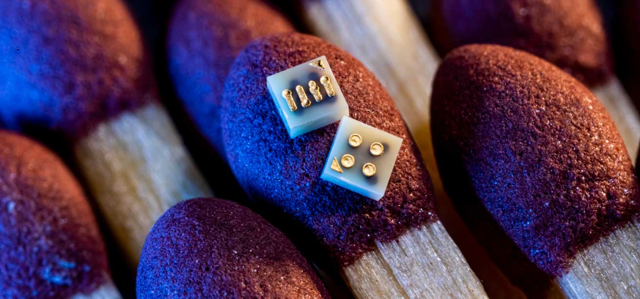
The AT&S Hardware Design Team from AIS (Advanced Interconnect Solution Services) created the layout of the circuit board. The connection design was made using the Embedded component packaging (ECP) technology implemented. This enables active and passive components to be integrated in laminate-based substrates, i.e. high-tech printed circuit boards, in the smallest of spaces.
“Instead of placing the components on the circuit board, they are integrated into the circuit board. They practically disappear inside the circuit board, ”says Mr. Maier. In addition, the Naneye project is an example of future products that AT&S will offer more frequently. "This product fits perfectly into our strategy and also shows where our journey will go," explains Gunter Kole, Director Advanced Interconnect Solution Service at AT&S. "In the future, we will not only develop connection solutions that have made us one of the global technology leaders, but we will also become a provider of complete solutions," says Günter Köle.
Camera module with chip on tip approach
The camera module uses a so-called chip on tip approach, in which Optics and image sensor be placed at the tip of the device or the distal end. The result is a significantly better image quality than when the camera module is at the other, proximal end. The Naneyem is a fully integrated imaging module. Thanks to its multi-element optics at wafer level, it delivers high-quality images. It has been specially developed for optimal performance over short distances.
 Vision Sensor solves many tasks in factory automation
The lens combines a wide field of view FoV with an extended depth of field DOF. It reduces distortion and provides a sharp, accurate picture. The digicam has a digital serial interface for Low Voltage Differential Signaling (LVDS). This enables a high signal-to-noise ratio (SNR). This means that the digicam can transmit images over long cable lengths without losing signal integrity and without increasing noise.
1 pixel sensitive sensors
The digicam offers a Frame rate up to 49 fps (Frames per second). The display is fluid and has little lag via a large number of standard interfaces with low power consumption. The image sensors are based on a pixel with high sensitivity. This is a lower one Lighting required and heat generation at the tip of the device is contained.
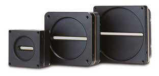 CMOS and CCD line scan cameras with maximum sensitivity
A pair of passendes Cables complements the camera module. It can be assembled up to a length of 3 m. The cable ensures smooth and seamless integration into the endoscopic device. At the tip of the camera, additional LEDs can make even less lighting necessary and keep heat generation under control. The fully digital output eliminates the cost of an external analog-to-digital conversion ADC because this is done on the chip. The camera module is less susceptible to magnetic interference from medical devices in surgery (EMI / EMC). This eliminates the need for coaxial cables or shielded cables.
General technical knowledge
What is Embedded Component Packaging?
embedded component packaging (ECP) is made possible by a special manufacturing process. First, the components are integrated into a resin layer in special manufacturing steps. Then the connection takes place through copper-filled, laser-drilled microvias. The embedded component dispenses with soldering points, while finer designs are possible on the outer layer. The components are also optimally protected against external influences. With ECP, more components can be integrated into the circuit board with the same size of the end device. This increases the functionality and leaves the circuit board with the same range of functionsshrink. More compact end devices are becoming feasible.
