MICROSYSTEM TECHNOLOGY
miniaturization and nanotechnology
Components in the micro range such as sensors, cameras, actuators for micro-fluidics, micro-mechanics and micro-optics
Image: AMS Osram

Here you will find components, systems and technologies for your development in microsystem technology, for miniaturization and the Nanotechnology such as sensors, actuators, microfluidics, micromechanics and micro-optics.
")
Microsystems technology is becoming more and more important for industry in the course of miniaturization, digitization and automation. Microsystems are composed of micromechanics, microelectronics, microfluidics and microoptics. Applications of microsystem technology can be found in Electrical Engineering and Medical Technology. It becomes even smaller with nanotechnology, which is an extension of microsystem technology. This is based on the proportions of the nanoparticles and takes place in the millionth of a millimeter. The lotus effect from bionics is probably one of the most famous applications here.
Discover Embedded and other solutions such as circuit board components, micromaterials and their processing, sensors and micro-optics for medical technology, Automotive industry, Consumer goods industry, among others:
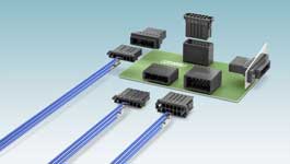 The crimp-based wire-to-board connectors Connexis has Phoenix Contact for the cable assembly designed in automated production. They allow fast and precise PCB connector. Optical identification on the connector makes assembly in the field or in-house production clear. The user can choose from a large number of individual prints.
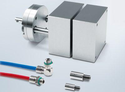
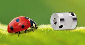 With the naked eye, the holes with a diameter of 1 mm or more are small Micro couplings from Orbit Drive Technology almost unrecognizable. Nevertheless, such a compensating coupling offers a performance that one might not expect from its tiny size. Their outer diameter can be compared to that of a ladybug and with their bore diameter they would fit into a larger spaghetti.
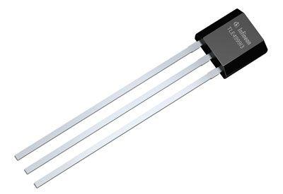 At the Sensor + Test trade fair, Infineon is the first semiconductor manufacturer to bring a monolithically integrated linear Hall sensor onto the market that has been developed entirely in accordance with the ISO26262 safety standard for automotive applications: the "Xensiv TLE4999I3" enables the development of fault-tolerant systems with just one component that must meet the highest requirement level for functional safety (ASIL D).
The extensive test capacities on the Coronavirus require automated analyzers. The efficiency in terms of test numbers, personnel and security is particularly important here. micropumps from HNP Microsystems help to run the processes in parallel and make them faster.

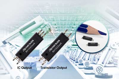 Renesas Electronic puts five new ones optocoupler with 8,2 mm creepage distance. They are the world's smallest insulation modules for industryautomation and Solar inverters. With a package width of 2,5 mm, the RV1S92xxA and RV1S22xxA reduce the PCB mounting area by 35% compared to products from other manufacturers.
 The smaller the workpiece, the more demanding the dimensional accuracy, this is especially true for use in the dental laboratory. Solid natural stone gives the micro machining center Zorn "Microone" the necessary stability. The Microone offers 5-axis simultaneous machining and CAM / CAD-made individual abutments for dental implant technology.
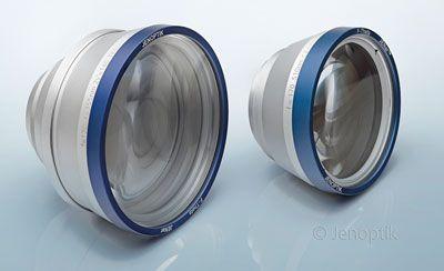 Jenoptik has expanded the “Jenar” F-Theta lens series for laser material processing to include a lens for the UV range: the F-Theta full quartz lens for 355 nm applications, with a focal length of 56 mm and a scan field of 22 mm, makes a lot possible small spot diameters down to 4,5 µm. It is specially designed for use in micro material processing and is suitable for applications with ultra-short pulses.
Framos offers with the new OLED microdisplay ECX335S series from Sony Semiconductor Solutions a solution that is suitable for the fast growing market of Augmented Reality (AR) devices. They are used in e.g. B. Head Mounted Displays (HMD), electronic viewfinders (VF) and as small monitors.

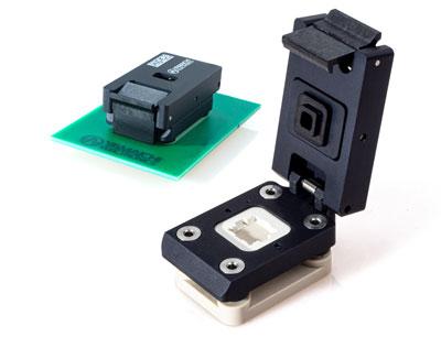 The new generation "Y-RED" is a completely revised further development of the semiconductor test contactors. It expands the Yamaichi Electronics product portfolio. It combines high-quality technology, standardized elements and simple and user-friendly assembly.
TDK Corporation is expanding its portfolio of Micronas linear Hall-effect sensors with the programmable HAL 1890. The new entry-level magnetic field sensor has a Sent output.
 Meusburger is now offering ready-to-install microforms with extensive accessories. The mold assemblies for micro injection molding are especially suitable for use in baby plastic machines and are available in different mold assembly variants. Ready-to-install ejector package systems with precise positioning of the ejectors and ideal guidance are available in two different versions from stock. This means that two unique, standardized solutions are available.
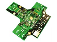 Beta Layout now offers HAL as a surface as well as chemical nickel / gold (Enig - Electroless Nickel Immersion Gold) for super flat pads in the PCB pool. With layer thicknesses of 4 to 8 µm nickel and 0,07 to 0,1 µm gold, the Enig surface is characterized by high planarity, good aging stability, suitability for soft soldering and bonding and as a surface for simple contact tasks. Electroless nickel / gold surfaces can be soldered several times and are often used in applications with very fine structures, which are becoming more common due to the miniaturization of components.